Shanghai Gengyun Industrial Co., Ltd
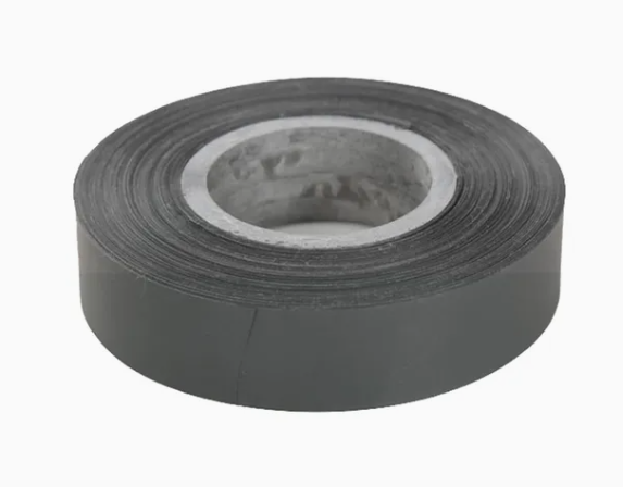
What is a semiconductor nylon tape with a shielding interval of 0.1mm
In the fields of high-speed communication, precision electronics, and high reliability power transmission, the requirements for electromagnetic compatibility (EMC), mechanical strength, and environmental
adaptability of cables and harnesses are becoming increasingly stringent. The semiconductor nylon tape with a shielding interval of 0.1mm, with its ultra precision structural design and material innovation, has become a breakthrough solution to solve complex electromagnetic interference and improve cable
protection level. This product adopts a unique composite design of “semiconductor layer+ultra dense
shielding mesh+nylon substrate”, which combines multiple functions such as conductivity, shielding, water resistance, and weather resistance, providing a new idea for high-end cable manufacturing. The following analysis will be conducted from three aspects: technical characteristics, application advantages, and industry value.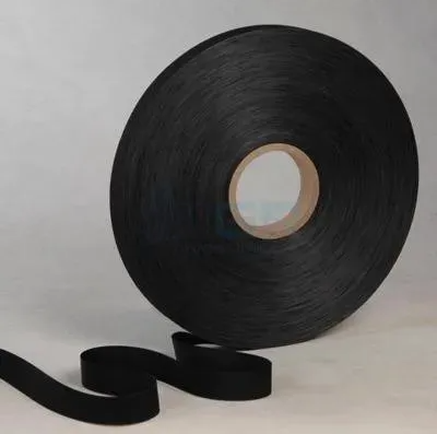
Ultra precision shielding interval design, reshaping electromagnetic protection performance
0.1mm nylonTraditional shielding materials, such as metal braided tape or aluminum foil, are prone to electromagnetic leakage during high-frequency signal transmission due to their large shielding gap
(usually ≥ 0.5mm), resulting in signal distortion or equipment interference. The semiconductor nylon tape with a shielding interval of 0.1mm is used to construct a uniformly distributed conductive grid on the
nylon substrate through precision etching technology, with a spacing accuracy of micrometer level, breaking through the traditional process limit:
-High frequency shielding efficiency doubling: 0.1mm ultra dense grid forms a continuous conductive layer, which can improve the reflection and absorption efficiency of electromagnetic waves to over 95% (test frequency range 1GHz~40GHz), especially suitable for high-frequency scenarios such as 5G base stations and millimeter wave radar.
-Lightweight and flexible balance: Compared to metal shielding layers, nylon substrates are 60% lighter and can withstand over 100000 bending tests, meeting the flexible wiring needs of miniaturized cables such as robot joint wires and medical endoscope wires.
tape-Corrosion resistance and environmental aging resistance: The semiconductor layer is made of nano carbon based composite materials, which have excellent salt spray resistance, acid and alkali resistance, and a service life that is more than three times longer than traditional metal shielding layers.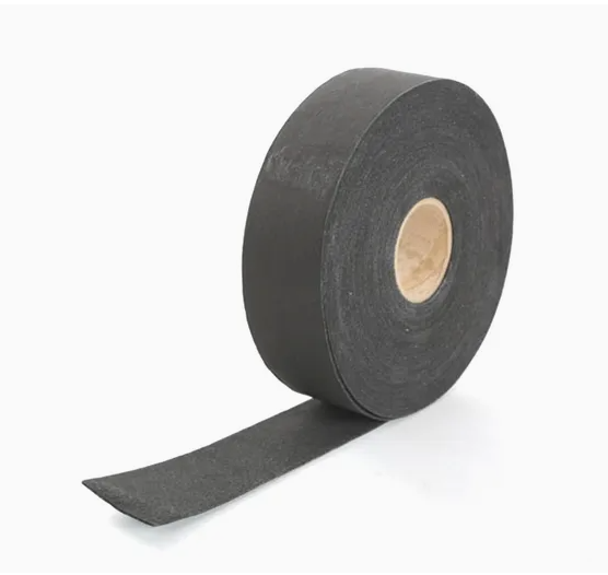
Empowering semiconductor characteristics to solve industry pain points
This material innovatively combines semiconductor characteristics with shielding function, overcoming problems such as poor grounding and static accumulation in traditional solutions
- Intelligent voltage equalization conductivity
The resistivity of the semiconductor layer is precisely controlled within the range of 10 ^ 4~10 ^ 6 Ω· cm, which can balance the surface electric field distribution of the cable, suppress partial discharge and corona effects, and reduce the insulation aging risk of high-voltage power cables (such as DC ± 500kV transmission systems). - Static dissipation and safety protection
The static decay time on the surface of the material is less than 0.1 seconds, which avoids spark discharge caused by charge accumulation and significantly improves safety in flammable and explosive environments (such as petrochemicals and energy storage power plants). - Integrated water and moisture resistance
Nylon substrate embedded with microporous water blocking structure, with a water expansion rate of up to 300%, and a longitudinal water blocking level that meets the highest requirements of IEC 60544-2 standard. It is suitable for high humidity scenarios such as submarine cables and outdoor photovoltaic power stations.
High process compatibility, significant cost reduction and efficiency improvement
This semiconductor nylon tape is fully compatible with modern cable manufacturing processes, helping enterprises achieve efficient production and green transformation:
-Automated bonding: Equipped with a pressure-sensitive adhesive layer, it supports seamless integration of high-speed wrapping equipment (line speed ≥ 50m/min), reducing manual intervention and increasing the yield rate to 99.5%.
-Environmental compliance: The materials are halogen-free and lead-free, compliant with RoHS 3.0 and EU REACH regulations, and meet the certification requirements of high-end fields such as automotive electronics (such as ISO 6722) and medical equipment.
-Whole life cycle cost optimization: temperature resistance range of -50 ℃~150 ℃, excellent UV resistance, outdoor service life of over 25 years, comprehensive operation and maintenance costs reduced by more than 40%.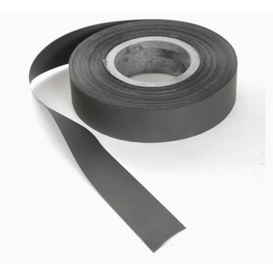
Multi scenario applications drive industry upgrading
- Communication field: 5G/6G base station antenna feeder, data center high-speed backplane connection line, ensuring signal integrity;
- In the field of new energy, high-voltage wiring harnesses for electric vehicles and DC cables for energy storage systems are used to solve electromagnetic interference and thermal management problems;
- Special equipment: aerospace cables, deep-sea exploration equipment, adapted to extreme temperature and pressure environments;
- Industrial automation: servo motors, flexible cables for industrial robots, enhance mechanical durability and anti-interference ability.
The semiconductor nylon tape with a shielding interval of 0.1mm redefines the performance boundary of cable shielding materials with its ultra precision structure, multifunctional integration, and high reliability.
Under the wave of intelligence and greenness, this material not only provides core support for equipment upgrades in fields such as communication, energy, and transportation, but also accelerates the cable
industry towards “high-density, high protection, and high compatibility”. In the future, with the continuous innovation of semiconductor technology and composite materials, their application scenarios are
expected to extend to cutting-edge fields such as quantum communication and space exploration, becoming one of the cornerstone materials for high-end manufacturing.
For further guidance or to explore our range of high-quality fiber optic solutions. Visit TOEM and MIC TOEM, optical communications is our specialty.